报告详情
Research On Two-Stage DC-DC Converter Suitable For High Voltage Input And Low Voltage Output
编号:57
访问权限:仅限参会人
更新:2024-10-22 15:35:55
浏览:175次
张贴报告
摘要
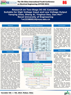
In this paper, a two-stage DC-DC converter topology is proposed to tackle the challenges of wide input range and high voltage levels in shipboard DC buses. A three-level Buck (TL Buck) converter is utilized as the front stage, thereby reducing the voltage stress on the MOSFETs to half of the input voltage. This makes it suitable for applications with high voltage levels and wide input ranges. Additionally, a star-connected three-phase LLC is employed as the rear stage to minimize output current ripple and achieve zero voltage switching (ZVS) and zero current switching (ZCS). A cascaded loop control with fixed frequency modulation strategy is adopted, demonstrating strong adaptability to wide input voltages. Finally, a simulation model is constructed to verify the correctness and feasibility of the proposed topology and control strategy.
关键词
High voltage input, soft switch, three-level Buck converter, three-phase LLC, two stage converter.
报告人

Yanqing Zhao
Student Naval University of Engineering稿件作者
全部评论
重要日期
-
会议日期
11月06日
2024
至11月08日
2024
-
09月15日 2024
初稿截稿日期
-
11月08日 2024
注册截止日期
主办单位
Huazhong University of Science and Technology
联系方式
历届会议
-
2023年12月08日 中国 Chengdu
4th China International Youth Conference on Electrical Engineering -
2023年07月11日 中国 Chengdu
2nd China International Youth Conference on Electrical Engineering -
2022年11月03日 中国 Wuhan
2022 IEEE 3rd China International Youth Conference on Electrical Engineering -
2020年11月02日 中国 Wuhan
China International Youth Conference on Electrical Engineering


发表评论